Shin-Etsu MicroSi Joins EV Group's Open Platform for Temporary Bonding Materials for 3D IC Manufacturing
New Platform Member Further Strengthens Supply Chain for EV Group's New ZoneBOND™ Capable EZR® (Edge Zone Release) and EZD® (Edge Zone Debond) Equipment Modules
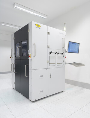
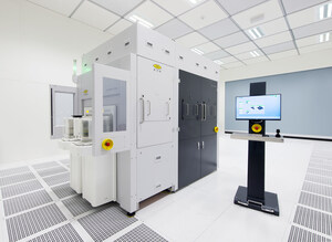
ST. FLORIAN, Austria and TOKYO, March 14, 2012 /PRNewswire/ -- EV Group (EVG), a leading supplier of wafer bonding and lithography equipment for the MEMS, nanotechnology and semiconductor markets, today announced that Shin-Etsu Chemical Co., Ltd., the world's largest supplier of semiconductor materials, has joined EVG's open platform for temporary bonding/debonding (TB/DB) materials. Shin-Etsu's advanced adhesives will be qualified with EVG's EZR® (Edge Zone Release) and EZD® (Edge Zone Debond) modules, which support the new ZoneBOND™ room temperature debonding process used in the production of 3D ICs.
"We are proud to be a partner in EVG's open platform for temporary bonding and debonding materials. Having worked closely with EVG's process development teams, we are pleased to have successfully completed the stringent test procedures for their ZoneBOND™ equipment. We look forward to working with customers that require temporary bonding to commercialize 3D packaging in a volume manufacturing environment," stated Jim Edmonds, president, Shin-Etsu MicroSi, Inc.
Markus Wimplinger, EVG's corporate technology development and IP director, commented, "Through our open materials platform approach, we are building a strong supply chain for EVG's market-leading TB/DB technologies—unlocking another key barrier in the advancement of 3D IC commercialization. Enabling the use of a wide range of adhesives from various suppliers for our equipment gives customers the most flexible choice of bonding materials for increased flexibility during thin wafer processing."
ZoneBOND™ capable technology, in tandem with EVG's breakthrough EZR® (Edge Zone Release) and EZD® (Edge Zone Debond) modules, provides a superior approach for temporary wafer bonding, thin wafer processing, and debonding applications—overcoming the last remaining limitations associated with thin wafer processing. Benefits of EVG's TB/DB equipment solutions and open materials platform include: the use of silicon, glass and other carriers; compatibility with existing, field-proven adhesive platforms; and the ability to debond at room temperature with virtually no vertical force being applied to the device wafer. To support grinding and backside processing at high temperatures and to allow for low-force carrier separation, the concept defines two distinctive zones on the carrier wafer surface with strong adhesion in the perimeter (edge zone) and minimal adhesion in the center zone. As a result, low separation force is only required for carrier separation once the polymeric edge adhesive has been removed by solvent dissolution or other means.
For further insight into the ZoneBOND™ approach, please view the recent webcast "3D is a Reality in High-volume Manufacturing" hosted by Yole Developpement available at: http://www.i-micronews.com/consult_webcast.asp?uid=63
About Shin-Etsu Chemical Co., Ltd.
Shin-Etsu Chemical Co., Ltd., the Tokyo based chemical company, is the world's largest supplier of semiconductor materials, semiconductor silicon, PVC resin, synthetic quartz glass and methylcellulose and is a major producer of materials including silicones and rare earth magnets. Shin-Etsu Chemical's stock (TSE: 4063) is listed on three markets: The Tokyo, Osaka and Nagoya Exchanges in Japan. http://www.shinetsu.co.jp
Shin-Etsu MicroSi, Inc. is a wholly owned subsidiary of Shin-Etsu Chemical Co., Ltd. With its headquarters in Phoenix, Arizona, Shin-Etsu MicroSi provides high performance products and materials, specifically designed to address today's photolithography, packaging, solar and flexible printed circuit requirements. www.microsi.com
About EV Group (EVG)
EV Group (EVG) is a world leader in wafer-processing solutions for semiconductor, MEMS and nanotechnology applications. Through close collaboration with its global customers, the company implements its flexible manufacturing model to develop reliable, high-quality, low-cost-of-ownership systems that are easily integrated into customers' fab lines. Key products include wafer bonding, lithography/nanoimprint lithography (NIL) and metrology equipment, as well as photoresist coaters, cleaners and inspection systems.
In addition to its dominant share of the market for wafer bonders, EVG holds a leading position in NIL and lithography for advanced packaging and MEMS. Along these lines, the company co-founded the EMC-3D consortium in 2006 to create and help drive implementation of a cost-effective through-silicon via (TSV) process for major ICs and MEMS/sensors. Other target semiconductor-related markets include silicon-on-insulator (SOI), compound semiconductor and silicon-based power-device solutions.
Founded in 1980, EVG is headquartered in St. Florian, Austria, and operates via a global customer support network, with subsidiaries in Tempe, Ariz.; Albany, N.Y.; Yokohama and Fukuoka, Japan; Seoul, Korea and Chung-Li, Taiwan. More information is available at www.EVGroup.com.
SOURCE EV Group


Share this article