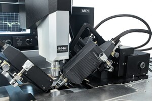
MPI Corporation Introduces New 300 mm Fully-Automatic TS3500 Wafer Probe Systems Series with WaferWallet (TM)
HSINCHU, Taiwan, Nov. 14, 2018 /PRNewswire/ -- MPI Corporation introduces a new 300 mm fully-automatic TS3500 wafer probe systems series with WaferWallet™.
Over the past decade, the semiconductor industry has been challenged with increasing demands for accurate on-wafer measurements for Device Characterization during the Modeling and New Technology Development processes. Current 300 mm solutions compromise on either measurement accuracy or automation capabilities. Overcoming these challenges, MPI now introduces the TS3500 probe station series configurable with unique MPI WaferWallet™ making it the most advanced fully-automatic system on the market. The combined capabilities now offer the customer unequaled measurement flexibility with test automation while significantly reducing the overall cost of test. MPI's WaferWallet™ also incorporates simple and convenient handling of multiple wafer types and sizes.
Common practice for Device Characterization in the Modeling and New Technology Development processes is to extract data from a typical few wafers via extremely accurate IV-CV, 1/f, RF, mmW, and Load-Pull measurements. MPI's WaferWallet™ extends the TS3500 series automation without compromising measurement capability. The WaferWallet™ is designed with five individual trays for manual, ergonomic loading of 150, 200, or 300 mm "modeling" wafers. Fully-Automated tests with up to five identical wafers at different temperatures are now possible.
"The TS3500 and TS3500-SE are equivalent in features to MPI's well-known and established TS3000 and TS3000-SE 300 mm probe stations with the added fully-automated capability by configuring or upgrading with MPI's unique WaferWallet™." Says Stojan Kanev, General Manager of MPI Corporation's Advanced Semiconductor Division. "MPI's solution is lowering the customer's overall cost-of-test by providing full automation for less than other vendor's semi-automated products."
The WaferWallet™ concept is another example of MPI leading the market by listening carefully to customer requirements and quickly turning ideas into valuable solutions.
About MPI Corporation
Founded in 1995 and headquartered in Hsinchu, Taiwan, MPI Corporation is a global technology leader in Semiconductor, Light Emitting Diode (LED), Photo Detectors, Lasers, Materials Research, Aerospace, Automotive, Fiber Optic, Electronic Components and more. MPI's four main business sectors include Probe Card, Photonics Automation, Advanced Semiconductor Test and Thermal Divisions. MPI products range from various advanced probe card technologies, probers, testers, material handlers, inspection and thermal air systems. Many of these products are accompanied by state-of-the-art Calibration and Test & Measurement software suites. The diversification of product portfolio and industries allows a healthy environment for employee growth and retention. Cross pollination of divisional product technologies stimulates MPI product innovations that are meaningful to our precious customer base.
SOURCE MPI Corporation


Share this article