Leti Orders HERCULES NIL System from EV Group for Joint Nanoimprint Lithography Program
NIL system will bolster process development and demo capabilities of INSPIRE program
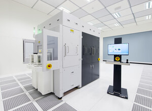
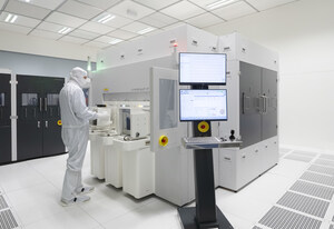
ST. FLORIAN, Austria and GRENOBLE, France, Sept. 21, 2016 /PRNewswire/ -- EV Group (EVG), a leading supplier of wafer bonding and lithography equipment for the MEMS, nanotechnology and semiconductor markets, and Leti, an institute of CEA Tech, announced today that Leti has ordered a HERCULES NIL track system from EV Group. The HERCULES NIL system will be installed in Leti's cleanroom facility in Grenoble, where it will augment the process-development and demonstration capabilities available to participants in the collaborative EVG-Leti INSPIRE program.
More than an industrial partnership to develop NIL process solutions, the INSPIRE program was launched by Leti and EVG in June 2015 to demonstrate the cost-of-ownership benefits of NIL for a wide range of application areas, such as photonics, plasmonics, lighting, photovoltaics, wafer-level optics and bio technology. Through INSPIRE, Leti and EVG are supporting the development of new applications from the feasibility-study stage to the first manufacturing steps on EVG platforms, as well as transferring integrated process solutions to their industrial partners. The result of this effort is to significantly lower the barriers for adopting NIL technology for use in manufacturing novel products.
"Nanoimprint lithography has shown significant potential as a low-cost, high-resolution patterning solution for emerging and growing applications outside the semiconductor industry," said Laurent Pain, patterning program manager, Leti. "The INSPIRE program launched by Leti and EVG is designed to accelerate the adoption of this promising technology in high-volume manufacturing. Installing this tool supports our goal of expanding and accelerating the scope of INSPIRE and demonstrating the benefits of this versatile, powerful nano-patterning technology."
"We are extremely pleased with the success of the INSPIRE program since Leti and EVG launched it one year ago," stated Markus Wimplinger, corporate technology development and IP director, EV Group. "To date, this program is supporting the development of NIL solutions for several customers thanks to the combined expertise and capabilities provided by both organizations. With the addition of EVG's HERCULES NIL track system—which has already been installed in multiple high-volume manufacturing sites—we expect INSPIRE's success to continue to grow."
HERCULES NIL is a fully integrated track system that combines cleaning, resist coating and baking pre-processing steps with EVG's proprietary SmartNIL™ large-area NIL process in a single platform. It can imprint structures in sizes ranging from tens of nanometers up to several micrometers while offering unmatched throughput (40 wph for 200-mm wafers). The system is built on a highly configurable and modular platform that accommodates a variety of imprint materials and structure sizes—providing a high degree of flexibility in addressing customers' manufacturing needs. The fully integrated approach also minimizes the risk of particle contamination.
About Leti (France)
As one of three advanced-research institutes within the CEA Technological Research Division, Leti serves as a bridge between basic research and production of micro- and nanotechnologies that improve the lives of people around the world. It is committed to creating innovation and transferring it to industry. Backed by its portfolio of 2,800 patents, Leti partners with large industrials, SMEs and startups to tailor advanced solutions that strengthen their competitive positions. It has launched 59 startups. Its 8,500m2 of new-generation cleanroom space feature 200mm and 300mm wafer processing of micro and nano solutions for applications ranging from space to smart devices. With a staff of more than 1,900, Leti is based in Grenoble, France, and has offices in Silicon Valley, Calif., and Tokyo. Follow us on www.leti.fr and @CEA_Leti.
About EV Group (EVG)
EV Group (EVG) is a leading supplier of equipment and process solutions for the manufacture of semiconductors, microelectromechanical systems (MEMS), compound semiconductors, power devices and nanotechnology devices. Key products include wafer bonding, thin-wafer processing, lithography/nanoimprint lithography (NIL) and metrology equipment, as well as photoresist coaters, cleaners and inspection systems. Founded in 1980, EV Group services and supports an elaborate network of global customers and partners all over the world. More information about EVG is available at www.EVGroup.com.
| Leti Press contact |
|
| Agency |
|
| Tel: +33 6 74 93 23 47 |
|
| E-mail: [email protected] |
|
| EV Group Contacts: |
|
| Clemens Schütte |
David Moreno |
| Director, Marketing and Communications |
Vice President |
| EV Group |
MCA, Inc. |
| Tel: +43 7712 5311 0 |
Tel: +1.650.968.8900, ext. 125 |
| E-mail: [email protected] |
E-mail: [email protected] |
SOURCE EV Group


Share this article