Korean National Nanofab Center Installs High-Vacuum Wafer Bonder from EV Group for Advanced MEMS Research and Foundry Services
High-vacuum capability of EVG520IS wafer bonder ideally suited for MEMS applications
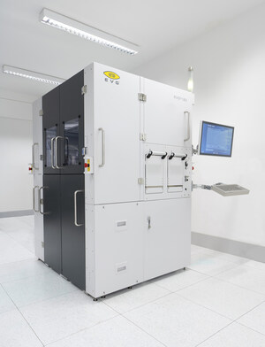
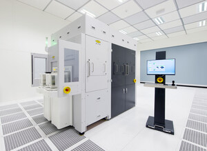
ST. FLORIAN, Austria, Jan. 26, 2016 /PRNewswire/ -- EV Group (EVG), a leading supplier of wafer bonding and lithography equipment for the MEMS, nanotechnology and semiconductor markets, today announced that it has supplied an EVG520IS semi-automated wafer bonding system with high-vacuum capability to the National Nanofab Center (NNFC), based in Daejeon, Korea. An affiliate of the Korea Advanced Institute of Science and Technology (KAIST), the NNFC has already installed the EVG520IS wafer bonder at its fab and is using it for advanced MEMS research and foundry services. The vacuum capability of the EVG system (up to 5x10⁻⁶ mbar) makes it ideally suited for MEMS applications that require a high-vacuum environment be maintained in the cavity after bonding, such as gyroscopes and micro-bolometers.
"NNFC's vision is to provide the critical infrastructure needed to support world-class nanotechnology research and business development. To that end, it is important that we have state-of-the-art process technology to support our key areas of research and foundry services, which include silicon CMOS, biochip technologies, nano-materials and MEMS," stated Dr. H.Y. Kim, department head of nanosystem research at NNFC. "EV Group is a recognized leader in wafer bonding, which is an enabling technology for advanced MEMS R&D and manufacturing. This recent purchase of the EVG520IS wafer bonder will enable us as well as our partners and customers to have ready access to process technology that is critical to advanced MEMS R&D and production."
For several decades, EVG has had a strong presence in Korea working closely with local device manufacturers, academia and research institutes in the micro- and nanoelectronics industries. EV Group Korea Ltd. was founded as a wholly owned subsidiary in 2008 to further improve and enhance local support for EVG's customers and partners. In addition to local sales, customer support, field service and spare parts management teams, EV Group Korea has its own technology development and process technology teams.
"EVG has a long history of partnering with academia and research institutes, like KAIST and the NNFC, which are at the leading edge of developing new processes and technologies that drive the micro-electronics and nanotechnology industries," stated Paul Lindner, executive technology director at EV Group. "These collaborations are an important part of our strategy of identifying opportunities where our process solutions can play an enabling role in developing new micro- and nanotechnology end-products and applications. We're pleased to offer our products and services to the NNFC in support of our shared mission and vision of furthering nanotechnology development, education and commercialization."
The EVG520IS is configurable for all wafer bonding processes, including anodic, thermo compression, fusion bonding, and low-temperature (LowTemp™) plasma bonding. More information is available at http://www.evgroup.com/en/products/bonding/waferbonding/evg520is/.
About EV Group (EVG)
EV Group (EVG) is a leading supplier of equipment and process solutions for the manufacture of semiconductors, microelectromechanical systems (MEMS), compound semiconductors, power devices and nanotechnology devices. Key products include wafer bonding, thin-wafer processing, lithography/nanoimprint lithography (NIL) and metrology equipment, as well as photoresist coaters, cleaners and inspection systems. Founded in 1980, EV Group services and supports an elaborate network of global customers and partners all over the world. More information about EVG is available at www.EVGroup.com.
SOURCE EV Group


Share this article