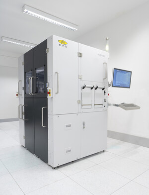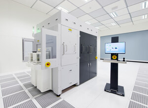
EVG Unveils EVG520L3 Next-Generation Wafer Bonding System with Key Cost-of-Ownership Advantages for Advanced Packaging and MEMS Applications
New Wafer Bonder from EVG Enables 3-5x Throughput Improvement for Breakthrough Cost-of-Ownership Performance
DRESDEN, Germany, Oct. 19 /PRNewswire/ -- SEMICON EUROPA — EV Group (EVG), a leading supplier of wafer-bonding and lithography equipment for the advanced semiconductor and packaging, MEMS, silicon-on-insulator (SOI) and emerging nanotechnology markets, today announced the latest addition to its industry-leading EVG500 Series of permanent wafer bonding systems. The new three-chamber EVG520L3 wafer bonding system builds on the series' proven strengths in temperature control, piston force uniformity and modularity, with the next major implementation of the bond chamber concept—addressing the need for high-vacuum, CMOS-compatible bonding processes while delivering significantly higher throughput, cost of ownership (CoO) and yields.
Ongoing industry exploration of new technologies for MEMS devices and advanced packaging/3D interconnect applications is driving increased demand for flexible, yet reliable, processing equipment. Wafer stacking and bonding systems must be able to accommodate a variety of materials and material properties, offer faster heating and cooling, and enable parallel processing capabilities to ensure overall quality and uniformity. The EVG520L3 was developed with these requirements in mind, delivering capabilities superior to those of competitive offerings—all the while addressing advanced CoO and yield requirements.
One of the most significant hurdles to higher throughput is long pumping times for achieving high vacuum in the device. To address this, the EVG520L3 features a brand new three-chamber design, which enables processing of up to three substrate stacks simultaneously. This concept utilizes pre- and post-bond process chambers, which separates the baking and pumping, high-vacuum bonding and post-bond cooling. The new layout speeds up the bond process (by up to 3x for high-vacuum and 5.5x for ultra-high vacuum), and results in significantly improved throughput and yield.
Other enhancements include:
- A heater design that supports 45 degrees C/minute heating and up to 100 degrees C/minute cooling ramps with silent wafer cooling, for improved temperature uniformity in EVG's proven heater design
- Rapid vacuum build-up to enable high-vacuum applications, such as bolometers
- Option to support up to 100kN contact force—enabling metallic bonds on the larger substrates used for MEMS and 3D IC applications
- Unparalleled force accuracy and uniformity for highest yield
Noted Paul Lindner, EVG's executive technology director, "We developed the EVG520L3 over several years as part of a global innovation effort driven by customers' feedback on their next-generation bonding requirements. The system's highly stable design has minimal moving parts inside the chamber, while the bonding module is fully compatible with our EVG540 single-chamber and Gemini integrated wafer bonding systems. Moreover, the bond chucks are compatible with our Gemini and EVG600 Series aligners. Together, these capabilities allow us to help our customers achieve both faster time to market and lower overall cost of ownership for their wafer bonding processes."
The EVG500 Series is designed for volume manufacturing of advanced packaging, 3D interconnect and MEMS applications, and performs all wafer bonding techniques utilizing EVG's unique process separation principle. Various wafer sizes and materials with modular configurations for easy transfer of R&D processes to production are supported. EVG's wafer bonding equipment achieves the highest yields for aligned wafer bonding in the industry.
"Wafer bonding is a critical process step in the manufacturing of 3D stacked chips and MEMS devices. As the rising design complexity and integration of new materials for these products drives up cost per wafer, manufacturers must not only meet tough yield and throughput requirements but also adhere to amazing cost pressures for high volume manufacturing," commented Principal Research Analyst, Mark Stromberg, of Gartner, Inc. "As a result, there is a clear critical need for a wafer bonding solution that can address all of these challenges."
Further supporting its expertise in the MEMS sector, EVG announced another key order for the MEMS market today—Norway-based MEMS sensor producer Sensonor Technologies AS ordered an EVG Gemini for thermal imaging manufacturing. Also at SEMICON Europa, EVG today announced that Fraunhofer ENAS has purchased an EVG6200NT automated mask aligner and an EVG540 automated wafer bonder, incorporating EVG's new SMS-NIL technology for ultra-high-resolution patterning.
Those interested in learning more about the new three-chamber EVG520L3 wafer bonding system and EV Group's broad portfolio of wafer bonding and lithography equipment are invited to visit the company in booth #1568 (Hall 1) during SEMICON Europa, October 19-21, 2010, at Messe Dresden, Dresden, Germany.
About EV Group
EV Group (EVG) is a world leader in wafer-processing solutions for semiconductor, MEMS and nanotechnology applications. Through close collaboration with its global customers, the company implements its flexible manufacturing model to develop reliable, high-quality, low-cost-of-ownership systems that are easily integrated into customers' fab lines. Key products include wafer bonding, lithography/nanoimprint lithography (NIL) and metrology equipment, as well as photoresist coaters, cleaners and inspection systems.
In addition to its dominant share of the market for wafer bonders, EVG holds a leading position in NIL and lithography for advanced packaging and MEMS. Along these lines, the company co-founded the EMC-3D consortium in 2006 to create and help drive implementation of a cost-effective through-silicon via (TSV) process for major ICs and MEMS/sensors. Other target semiconductor-related markets include silicon-on-insulator (SOI), compound semiconductor and silicon-based power-device solutions.
Founded in 1980, EVG is headquartered in St. Florian, Austria, and operates via a global customer support network, with subsidiaries in Tempe, Ariz.; Albany, N.Y.; Yokohama and Fukuoka, Japan; Seoul, Korea and Chung-Li, Taiwan. The company's unique Triple i-approach (invent - innovate - implement) is supported by a vertical integration, allowing EVG to respond quickly to new technology developments, apply the technology to manufacturing challenges and expedite device manufacturing in high volume. More information is available at www.EVGroup.com.
SOURCE EV Group


Share this article