EV Group Signs Collaboration Agreement with Eulitha to Establish Low-Cost-of-Ownership Nanopatterning Solution For HB-LED Manufacturing
ST. FLORIAN, Austria, Jan. 10, 2012 /PRNewswire/ -- EV Group (EVG), a leading supplier of wafer bonding and lithography equipment for the MEMS, nanotechnology and semiconductor markets, today announced that it has signed a joint-development and licensing agreement with Eulitha AG, a pioneer and leader in the production of high-quality nanostructures using advanced lithography techniques. EVG will integrate Eulitha's PHABLE™ mask-based ultraviolet (UV) photolithography technology with EVG's automated mask aligner product platform with the goal of developing a low-cost-of-ownership (CoO) nanopatterning solution to enable the production of high-brightness light emitting diodes (HB-LEDs). With demo capabilities in place already, the first products are expected to ship later this year.
(Photo: http://photos.prnewswire.com/prnh/20120110/SF30748)
According to LED market research firm Strategies Unlimited (Mountain View, Calif.), the market for high-brightness LEDs is expected to grow from $11.2 billion in 2010 to $16.2 billion in 2014, driven by applications such as TV backlighting, mobile devices and increasingly by lighting. To meet this increased demand, LED manufacturers need new manufacturing solutions that can increase the lighting efficiency of their products while keeping manufacturing costs down. Through their joint-development agreement, EV Group and Eulitha will explore new manufacturing technologies that support LED manufacturers' cost and technology requirements.
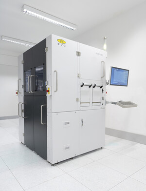
Combining Eulitha's full-field exposure technology with EVG's well-established mask alignment platform provides low-cost, automated fabrication of photonic nanostructures over large areas, and supports the production of energy efficient LEDs, solar cells and liquid crystal displays. It combines the low cost, ease-of-use and non-contact capabilities of proximity lithography with sub-micron resolution—making it ideally suited for use in patterning sapphire substrates in order to enhance the light extraction (and thus the efficiency) of LED devices. EVG plans to offer a PHABLE-enabled EVG620 system as an extension to its well-established mask alignment system platform—giving customers an even wider choice of configuration options.
"We look forward to working with EV Group to greatly accelerate commercialization of PHABLE through the integration of this novel technology with EVG's industry-leading mask aligner platform," stated Harun Solak, CEO of Eulitha. "We believe the synergies of our respective technologies have great potential to provide the resolution and volume-production capabilities of lithography steppers at a fraction of the cost—enabling LED, optics and photonics manufacturers with extremely tight cost constraints the opportunity to extend their technology roadmaps to higher levels of performance."
Noted Hermann Waltl, executive sales and customer support director, EV Group, "Eulitha's expertise in nanofabrication makes them an ideal partner to collaborate with on new patterning solutions for the LED industry. We are excited to embark on this relationship with Eulitha and advance our proven mask aligner platform for our LED customers."
About Eulitha
Eulitha AG is a spin-off company of the Paul Scherrer Institute, Switzerland. It specializes in the development of innovative lithographic technologies for applications in optoelectronics, photonics, biotechnology, and data storage. It produces and markets nano-patterned wafers and templates using its unique EUV interference method and state-of-the-art e-beam lithography tools. PHABLE is the brand name of its new photolithography platform, which includes exposure tools and wafer patterning services. For more information about Eulitha, please visit www.eulitha.com.
About EV Group
EV Group (EVG) is a world leader in wafer-processing solutions for semiconductor, MEMS and nanotechnology applications. Through close collaboration with its global customers, the company implements its flexible manufacturing model to develop reliable, high-quality, low-cost-of-ownership systems that are easily integrated into customers' fab lines. Key products include wafer bonding, lithography/nanoimprint lithography (NIL) and metrology equipment, as well as photoresist coaters, cleaners and inspection systems.
In addition to its dominant share of the market for wafer bonders, EVG holds a leading position in NIL and lithography for advanced packaging and MEMS. Along these lines, the company co-founded the EMC-3D consortium in 2006 to create and help drive implementation of a cost-effective through-silicon via (TSV) process for major ICs and MEMS/sensors. Other target semiconductor-related markets include silicon-on-insulator (SOI), compound semiconductor and silicon-based power-device solutions.
Founded in 1980, EVG is headquartered in St. Florian, Austria, and operates via a global customer support network, with subsidiaries in Tempe, Ariz.; Albany, N.Y.; Yokohama and Fukuoka, Japan; Seoul, Korea and Chung-Li, Taiwan. The company's unique Triple-i approach (invent - innovate - implement) is supported by a vertical integration, allowing EVG to respond quickly to new technology developments, apply the technology to manufacturing challenges and expedite device manufacturing in high volume. More information is available at www.EVGroup.com.
SOURCE EV Group


Share this article