EV Group Recognized as Leader in Nanoimprint Lithography With Frost & Sullivan 2010 Technology Innovation Award
ST. FLORIAN, Austria, April 11, 2011 /PRNewswire/ -- EV Group (EVG), a leading supplier of wafer bonding and lithography equipment for the MEMS, nanotechnology and semiconductor markets, today announced that it has received the 2010 European Nanoimprint Technology Product Innovation Award from independent market research firm, Frost & Sullivan. The prestigious award recognizes EVG's accomplishments in addressing industrial needs with nanoimprinting solutions.
Frost & Sullivan implemented a comprehensive research study that ranked multiple nanoimprint lithography (NIL) providers across several categories including advancement of technology, industrial implementation, solution portfolio, fulfilling future market needs, and impact on end user. EVG received among the highest marks in every category and ranked significantly higher than the nearest competitor overall.
"With market leadership in wafer bonding, 3D interconnect and MEMS manufacturing tools, EV Group has vast expertise in different areas that synergize with its nanoimprinting solutions," said Frost & Sullivan research analyst, Kenneth Chua. "The company is known to provide proven solutions fulfilling the needs of the semiconductor industry. Its NIL equipment continues this legacy and brings about low-cost, high-throughput and reliable solutions to its end-users."
According to Frost & Sullivan, much of the competition in NIL has been focused on making NIL viable for either mainstream semiconductor fabrication or patterning for future data storage media (bit patterned media in hard disk drives). In contrast, EVG has leveraged its expertise and experience to focus on key high-growth markets, including optics and microfluidics, where manufacturers are successfully benefiting from EVG's NIL technology today.
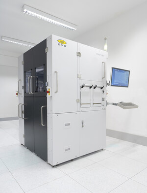
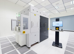
Moreover, as EVG continues to enhance the capabilities and performance of its NIL technology, it periodically evaluates its potential for other markets—and is prepared to realign its development strategies in the event that NIL becomes better suited to the needs of data storage and mainstream semiconductor manufacturers. This is evident in EVG's latest development, which is the ability to pattern features as small as 12.5 nm in diameter using ultraviolet-assisted nanoimprinting, compatible with its EVG620, EVG6200 and EVG770 NIL systems.
Commenting on the award, Dr. Thomas Glinsner, EV Group's head of product management said, "With a decade of experience in nanoimprint lithography, this award is testament to the quality and EVG's outstanding achievements in NIL technology innovation, as well as to the company's overall success in aligning its development efforts with market demand."
Nanoimprinting is used to produce patterns on a substrate by mechanical means. EVG's ultra-violet assisted NIL (UV-NIL) as well as hot embossing processes leverages the company's proprietary soft stamp technology, whereby a master imprinting stamp is used to generate soft stamps. This method increases the lifetime of the master stamp due to reduced mechanical contact and enables its customers to benefit from an overall reduction in cost of ownership. For more information about EV Group's complete nanoimprint lithography product portfolio, please visit http://www.evgroup.com/en/products/lithography/nil_systems/
About Frost & Sullivan
Frost & Sullivan, the Growth Partnership Company, enables clients to accelerate growth and achieve best-in-class positions in growth, innovation and leadership. The company's Growth Partnership Service provides the CEO and the CEO's Growth Team with disciplined research and best-practice models to drive the generation, evaluation, and implementation of powerful growth strategies. Frost & Sullivan leverages 50 years of experience in partnering with Global 1000 companies, emerging businesses and the investment community from more than 40 offices on six continents. To join our Growth Partnership, please visit http://www.awards.frost.com.
About EV Group
EV Group (EVG) is a world leader in wafer-processing solutions for semiconductor, MEMS and nanotechnology applications. Through close collaboration with its global customers, the company implements its flexible manufacturing model to develop reliable, high-quality, low-cost-of-ownership systems that are easily integrated into customers' fab lines. Key products include wafer bonding, lithography/nanoimprint lithography (NIL) and metrology equipment, as well as photoresist coaters, cleaners and inspection systems.
In addition to its dominant share of the market for wafer bonders, EVG holds a leading position in NIL and lithography for advanced packaging and MEMS. Along these lines, the company co-founded the EMC-3D consortium in 2006 to create and help drive implementation of a cost-effective through-silicon via (TSV) process for major ICs and MEMS/sensors. Other target semiconductor-related markets include silicon-on-insulator (SOI), compound semiconductor and silicon-based power-device solutions.
Founded in 1980, EVG is headquartered in St. Florian, Austria, and operates via a global customer support network, with subsidiaries in Tempe, Ariz.; Albany, N.Y.; Yokohama and Fukuoka, Japan; Seoul, Korea and Chung-Li, Taiwan. The company's unique Triple i-approach (invent - innovate - implement) is supported by a vertical integration, allowing EVG to respond quickly to new technology developments, apply the technology to manufacturing challenges and expedite device manufacturing in high volume. More information is available at www.EVGroup.com.
SOURCE EV Group


Share this article