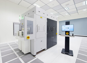
EV Group Optimizes Resist and Lithographic Processing for Plasma Dicing for Advanced Semiconductor Packaging Applications
EVG resist processing and lithography systems provide pre-processing solution to enable complete damage-free advanced dry plasma dicing on thin semiconductor wafers
ST. FLORIAN, Austria, June 20, 2017 /PRNewswire/ -- EV Group (EVG), a leading supplier of wafer bonding and lithography equipment for the MEMS, nanotechnology and semiconductor markets, today announced it is demonstrating optimized pre-processing solutions for the implementation of plasma dicing for advanced semiconductor packaging applications. EVG's latest products and process development services support this emerging semiconductor back-end fabrication process by protecting bumps and other topography with highly uniform resist layer and lithographic patterning of narrow dicing streets. By combining EVG's systems with third-party dry plasma dicing systems, customers can obtain a complete solution that will enable highly parallel, high-throughput, debris-free die singulation without risking bump reliability or impacting structured surfaces. EVG's offerings address the critical pre-processing requirements for mid-end-of-line (MEOL) and back-end-of-line (BEOL) processing of MEMS, power devices, RFID components, image sensors, logic and memory.
Thinner and smaller semiconductor chips are required to support the latest generation of mobile and wearable devices as well as to facilitate the Internet of Things (IoT). Plasma dicing offers numerous advantages for die singulation, such as reducing dicing street widths, providing flexible chip layouts as well as eliminating sidewall damage, chipping and wafer breakage. However, plasma dicing also brings new pre-process requirements, including the need for protecting top-side or bottom-side structures prior to singulation, conformal coating of severe topography features, thick resists for deep etching, and lithography to open up the dicing lanes.
EVG's high-quality, low cost-of-ownership resist processing and lithography systems address all of the pre-processing steps needed for advanced plasma dicing, including resist coating and development, as well as mask alignment lithography:
- EVG's proprietary OmniSpray® technology enables uniform coating of high-topography surfaces and bumps across the wafer—where traditional spin-coating techniques are limited—with sufficient thickness to fully protect bumps during plasma processing while providing the base for lithographic patterning of dicing streets.
- EVG's mask aligners provide optimal patterning quality with spray coating resists, including excellent depth of focus, high uniformity over topography, high throughput, and high resolution in deep cavities and trenches (down to 10µm even for large proximity gaps wider than 100µm), making them ideally suited to expose and open up the dicing lines.
- The pre-processing line is completed with EVG's high-throughput development systems.
- All systems can be provided in semi-automated and fully automated configurations, and are fully compatible with film-frame handling, making them ideally suited for die singulation in advanced packaging.
"The semiconductor industry is increasingly driving device performance through vertical stacking on thinner substrates. This trend is leading to greater demand not only for new wafer dicing technologies, but also for the supporting pre-processing equipment such as our coat, develop and mask alignment systems," stated Markus Wimplinger, corporate technology development and IP director at EV Group. "We are pleased to offer demonstrations of our complete line of R&D and volume-production pre-processing systems for plasma dicing at our demo labs in Austria, the U.S. and Japan, where customers can witness the yield and cost-of-ownership benefits of this powerful end-to-end wafer dicing solution for their custom advanced packaging needs."
EVG will also showcase its latest suite of lithography and resist processing solutions for advanced packaging applications at SEMICON West, to be held July 11-13 at the Moscone Convention Center in San Francisco, Calif. Attendees interested in learning more can visit EVG at Booth #7211 in the West Hall.
More information on EVG's lithography and resist processing solutions is also available at: https://www.evgroup.com/en/products/lithography/photolithography/
About EV Group (EVG)
EV Group (EVG) is a leading supplier of equipment and process solutions for the manufacture of semiconductors, microelectromechanical systems (MEMS), compound semiconductors, power devices and nanotechnology devices. Key products include wafer bonding, thin-wafer processing, lithography/nanoimprint lithography (NIL) and metrology equipment, as well as photoresist coaters, cleaners and inspection systems. Founded in 1980, EV Group services and supports an elaborate network of global customers and partners all over the world. More information about EVG is available at www.EVGroup.com.
| Contacts: |
|
| Clemens Schütte |
David Moreno |
| Director, Marketing and Communications |
Vice President |
| EV Group |
MCA, Inc. |
| Tel: +43 7712 5311 0 |
Tel: +1.650.968.8900, ext. 125 |
| E-mail: [email protected] |
E-mail: [email protected] |
SOURCE EV Group


Share this article