EV Group Completes Cleanroom Expansion, Opens New R&D Labs And Customer Training Center At Corporate Headquarters
Semiconductor Equipment Manufacturer Doubles Cleanroom Space and Advances on Long-term Growth Plans
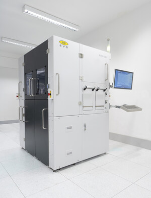
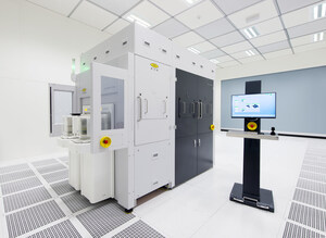
ST. FLORIAN, Austria, Nov. 27, 2012 /PRNewswire/ -- EV Group (EVG) a leading supplier of wafer bonding and lithography equipment for the MEMS, nanotechnology and semiconductor markets, announced the completion of its newly expanded cleanroom IV facility at its corporate headquarters in Austria. As part of the company's long-term growth strategy to address high-volume tool orders and speed time to market for its worldwide customer base, EV Group doubled its cleanroom space for process development and pilot production services. On top of that, the company increased the size of its application labs, added new R&D facilities for internal tool development and testing, and opened a new customer and employee training center.
In tandem with the new cleanroom expansion, EVG increased the number of fully automated high-volume manufacturing (HVM) systems (for different wafer sizes) to strengthen its customer demonstration and process development capabilities. While manufacturing and product development are centralized at EV Group's corporate headquarters, technology and process development teams in Austria work closely with the company's subsidiaries in Tempe, Arizona; Albany, New York; Yokohama and Fukuoka, Japan; Seoul, South Korea; and Chung-Li, Taiwan where additional, state-of-the-art application labs and cleanroom facilities are available for onsite customer demonstration and technology process development. EVG works closely with leading universities and R&D institutes worldwide, and plays a key role in numerous industry associations and consortia to contribute and continue the world's most advanced research and development for semiconductors, MEMS, light emitting diodes (LEDs) and other high-tech devices.
EV Group's new customer and employee training center at its corporate headquarters provides several new rooms for instructional training courses, as well as a large number of manual and automated EVG tools for training. This new training center provides EVG with additional flexibility and increased capability for customers and employees worldwide who regularly attend training courses on EVG technologies, manufacturing processes, products and software, as well as equipment operation.
Earlier this year, the addition of an ultra-modern manufacturing facility doubling the production floor space marked the completion of the first phase of EVG's long term expansion plans. Already positively contributing to EVG's continued, steady growth from the beginning of 2012, the company increased its order intake in fiscal year 2012 (ended September 30, 2012) by 5 percent over fiscal 2011—and increased its revenue by 20 percent within the same period. Additionally, in the last 12 months EVG added more than 100 new employees (to a current total of approximately 600 worldwide) and continues to recruit new employees in all departments.
About EV Group (EVG)
EV Group (EVG) is a leading supplier of equipment and process solutions for the manufacture of semiconductors, microelectromechanical systems (MEMS), compound semiconductors, power devices and nanotechnology devices. Key products include wafer bonding, thin-wafer processing, lithography/nanoimprint lithography (NIL) and metrology equipment, as well as photoresist coaters, cleaners and inspection systems. Founded in 1980, EV Group services and supports an extensive network of global customers and partners all over the world. More information about EVG is available at www.EVGroup.com.
SOURCE EV Group


Share this article