EV Group Breaks Through Resolution Barrier With Introduction of Soft UV Nanoimprint Lithography Technology
EVG's New SMS-NIL Technology Achieves Ultra-high-resolution Patterning Down to 12.5 nm
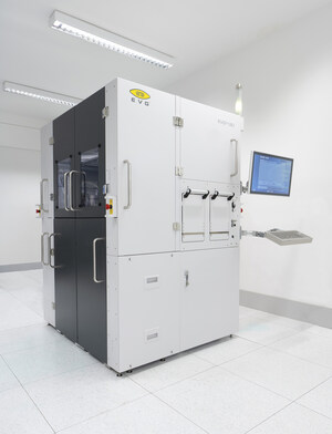
COPENHAGEN, Denmark, Oct. 13 /PRNewswire/ -- NNT CONFERENCE -- EV Group (EVG), a leading supplier of wafer bonding and lithography equipment for the MEMS, nanotechnology and semiconductor markets, today unveiled a new technology capability that enables ultra-high-resolution patterning of features down to 12.5 nm: Soft Molecular Scale Nanoimprint Lithography (SMS-NIL). Based on EVG's proven UV-NIL systems, SMS-NIL provides customers with a repeatable, cost-effective process for producing ultra-high-resolution patterning on large-area surfaces. Using the new technology's soft working stamp nanoimprint process, customers can perform full-area nanoimprints and optically aligned UV-NIL on existing EVG equipment. Likewise, the stamp and imprinting can be processed on the same tool without requiring additional processing steps—saving customers significant processing time and money.
UV-NIL offers a significantly lower processing cost than other nano-patterning techniques, making it an attractive solution for CMOS image sensors, micro lens molding and other optical applications where the technology is already being used. SMS-NIL takes this approach a step further, employing soft polymeric working stamps to avoid damaging costly master stamps. The stamp material's inherent properties greatly reduce the risk of mechanical damage to master templates, thus extending their lifetime. The working stamps' relatively low surface energy facilitates separation from the substrate after the imprinting process, while their flexibility allows the stamps to be used for multiple imprints.
Gerald Kreindl, product manager for nanoimprint lithography at EV Group, said, "For more than 10 years, we have maintained a strong technology focus on nanoimprint lithography and hot embossing. SMS-NIL is the culmination of our efforts to address customers' challenges in this area by creating the ultra-high-resolution patterning they need in a process that is repeatable and shows great promise for cost-effective high-volume manufacturing. This new technology capability is another step in EV Group's mission to enhance our existing technology solutions while pursuing cutting-edge research and development for new products and applications. This technology introduction is also an important step in commercializing nanoimprint lithography as a low-cost, high-throughput, ultra-high-resolution lithography technique."
EV Group offers two flexible purchase options for SMS-NIL. Customers who are interested in producing the working stamps in-house may purchase EV Group's process technology consultancy services to enable their own application development. EV Group also offers the option of purchasing working stamps ready for processing. The new technology is compatible with EVG's proven UV-based imprinting systems, including the EVG620, EVG6200, IQ Aligner and EVG770.
Those interested in learning more about EVG's SMS-NIL technology and broad portfolio of wafer bonding and lithography equipment are invited to visit the company during the Ninth International Conference on Nanoimprint and Nanoprint Technology (NNT), October 13-15, 2010, at First Hotel Skt. Petri, Copenhagen, Denmark.
About EV Group
EV Group (EVG) is a world leader in wafer-processing solutions for semiconductor, MEMS and nanotechnology applications. Through close collaboration with its global customers, the company implements its flexible manufacturing model to develop reliable, high-quality, low-cost-of-ownership systems that are easily integrated into customers' fab lines. Key products include wafer bonding, lithography/nanoimprint lithography (NIL) and metrology equipment, as well as photoresist coaters, cleaners and inspection systems.
In addition to its dominant share of the market for wafer bonders, EVG holds a leading position in NIL and lithography for advanced packaging and MEMS. Along these lines, the company co-founded the EMC-3D consortium in 2006 to create and help drive implementation of a cost-effective through-silicon via (TSV) process for major ICs and MEMS/sensors. Other target semiconductor-related markets include silicon-on-insulator (SOI), compound semiconductor and silicon-based power-device solutions.
Founded in 1980, EVG is headquartered in St. Florian, Austria, and operates via a global customer support network, with subsidiaries in Tempe, Ariz.; Albany, N.Y.; Yokohama and Fukuoka, Japan; Seoul, Korea and Chung-Li, Taiwan. The company's unique Triple i-approach (invent - innovate - implement) is supported by a vertical integration, allowing EVG to respond quickly to new technology developments, apply the technology to manufacturing challenges and expedite device manufacturing in high volume. More information is available at www.EVGroup.com.
SOURCE EV Group


Share this article