EV Group and IBM Sign License Agreement on Laser Debonding Technology
IBM's Hybrid Laser Release Process technology complements EV Group's low-temperature laser debonding equipment and process portfolio designed to enable highly flexible, high-throughput solution
ST. FLORIAN, Austria, March 14, 2018 /PRNewswire/ -- EV Group (EVG), a leading supplier of wafer bonding and lithography equipment for the MEMS, nanotechnology and semiconductor markets, and IBM (NYSE: IBM) today announced that the companies agreed to sign a license agreement on laser debonding technology. EVG plans to integrate IBM's patented Hybrid Laser Release process into EVG's advanced, field-proven temporary bonding and debonding equipment solutions, which can provide high-volume manufacturers with greater flexibility to implement optimized temporary bonding and debonding process flows. Thanks to the added process variants from IBM that will be supported by EVG's equipment portfolio, customers can choose from a wide range of bonding, cleaning and metrology process options to help address their temporary bonding and debonding requirements and applications.
The result, which is an advanced laser debonding solution based on EVG's combination of the technology licensed from IBM with EVG's know-how, encompasses methods and designs for UV and IR laser debonding (designed to enable the use of glass or silicon carriers) as well as inspection of the bond interfaces. The technologies contributed by IBM help EVG implement designs that address the industry's critical requirements for temporary bonding and debonding, including high throughput, low wafer stress for high yield, and low cost of ownership of the laser equipment, processing and consumables. The advanced EVG solution encompasses techniques to help protect chips from heat and laser damage, as well as chemical clean technologies for device and carrier wafers.
"This agreement with IBM enables EV Group to provide a comprehensive and flexible technology offering to our high-volume production customers that can enable them to produce value-added devices at greater flexibility, throughput and cost-efficiency," said Markus Wimplinger, EVG's corporate technology development and IP director.
"The laser debonding technology using glass or silicon carrier wafers can provide prototyping through high throughput manufacturing efficiency, a low cost of ownership, and a miniaturization platform. A growing range of fabrication demonstrations and applications supported include mobile phones, healthcare and IoT micro-systems, sensors and miniaturized size components handling, bio-sensors, bio-chips and diagnostics systems, and artificial intelligence solutions," said Dr. John Knickerbocker, Manager, Micro-Systems Technology & Solutions, IBM Research.
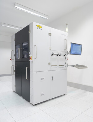
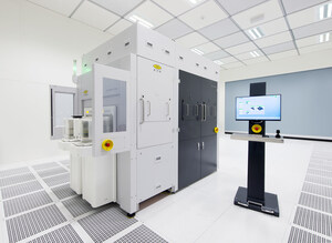
Designed for integration in the company's benchmark EVG®850DB automated debonding system, EVG's laser debonding modules incorporate a solid-state laser and proprietary beam-shaping optics designed to enable optimized, force-free debonding. Featuring both low-temperature debonding and high-temperature-processing stability, EVG's laser debonding solution is available for a variety of applications. These include fan-out wafer-level packaging (FO-WLP) and other temperature-sensitive processes such as memory stacking and integration, die-partitioning, heterogeneous integration and bio-technology / organic packages and devices applications, as well as photonics, compound semiconductors and power devices.
More information on EV Group's laser debonding solutions and the EVG850DB automated debonding system are also available at: https://www.evgroup.com/en/solutions/3d-ic/thin_wafer_processing/laser_initiated_debonding
About EV Group (EVG)
EV Group (EVG) is a leading supplier of equipment and process solutions for the manufacture of semiconductors, microelectromechanical systems (MEMS), compound semiconductors, power devices and nanotechnology devices. Key products include wafer bonding, thin-wafer processing, lithography/nanoimprint lithography (NIL) and metrology equipment, as well as photoresist coaters, cleaners and inspection systems. Founded in 1980, EV Group services and supports an elaborate network of global customers and partners all over the world. More information about EVG is available at www.EVGroup.com.
| EV Group Contacts: |
|
| Clemens Schütte |
David Moreno |
| Director, Marketing and Communications |
Principal |
| EV Group |
Open Sky Communications |
| Tel: +43 7712 5311 0 |
Tel: +1.415.519.3915 |
| E-mail: [email protected] |
E-mail: [email protected] |
SOURCE EV Group


Share this article