EV Group and Fraunhofer IZM-ASSID Establish Joint Development Agreement for High-Volume 3D Integration Applications
JDA to Extend Limits of Temporary Bonding/Debonding Technology to Support High-Topography Wafers and Chips
DRESDEN, Germany, Oct. 11, 2011 /PRNewswire/ -- SEMICON EUROPA - EV Group (EVG), a leading supplier of wafer bonding and lithography equipment for the MEMS, nanotechnology and semiconductor markets, today announced that it has established an agreement with world-renowned research institute Fraunhofer IZM-ASSID (All Silicon System Integration Dresden) to jointly develop high-volume manufacturing processes for 3D IC integration applications. Specifically, the two organizations will leverage their expertise to extend temporary bonding and debonding processes to support chip-to-wafer bonding with higher levels of topography (up to 600 microns thick)—a critical step in ramping 3D IC technology to volume production. The joint-development project will take place in ASSID's leading-edge facility in Dresden, Germany—the first Fraunhofer Center with a 300-mm line dedicated to developing processes for high-volume 3D IC manufacturing and prototyping.
"The growing need for 'More than Moore' approaches to extend semiconductor performance makes it ever-more important to develop and commercialize new processes to enable 3D IC integration," stated M. Jurgen Wolf, manager of Fraunhofer IZM-ASSID. "We look forward to strengthening our partnership with EVG to new levels as we work together to develop and optimize processes critical to enabling 3D IC production."
Chip-to-wafer bonding, where chips from one wafer are diced and joined to another wafer, has emerged as a promising method for enabling 3D IC integration. In chip-to-wafer bonding, chips can be tested before bonding to ensure that only known good die are joined together—enabling higher device yields. In addition, devices with heterogeneous technologies (different sizes, feature dimensions, etc.) can be bonded together to achieve 3D die stacks with a broad range of functionality (logic, memory, mixed signal, photonics, etc.) in the smallest possible space. Currently, the most advanced temporary bonding/debonding processes can support bonded wafers with topographies up to 100 microns thick. However, as the complexity of the die structures continues to increase, the topography of the bonded wafers will increase in thickness as well—requiring continuous advances in rigid backgrinding support for wafer thinning, as well as low vertical force debonding to avoid defects during the debonding process.
"As a leader in advanced semiconductor R&D, Fraunhofer IZM-ASSID is constantly pushing the envelope on new process technologies needed to keep the semiconductor industry on its roadmap," stated Markus Wimplinger, corporate technology development and IP director for EVG. "Their proven track record of delivering industrial solutions coupled with their expertise in wafer-level packaging makes them an ideal partner for jointly developing advanced processes, including temporary bonding and debonding, to accelerate the production of 3D ICs."
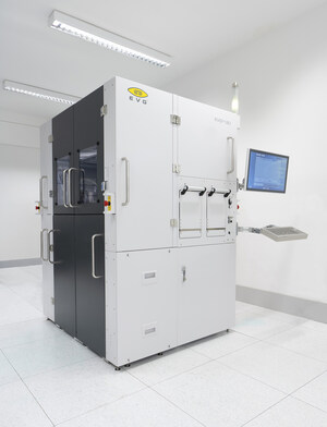
Under the terms of the agreement, EVG will provide its extensive expertise in 3D IC tooling and process development, particularly in wafer debonding. Fraunhofer IZM-ASSID will in turn lend its industry-leading expertise in wafer-level packaging and system integration technologies, access to test samples and demonstrator materials, and its established network with other research institutes and universities in the field of advanced system integration to ensure that the developed processes fully meet the industry's requirements for 3D process integration. Process development work will be accomplished using EVG850 TB/DB systems already installed at Fraunhofer IZM-ASSID's facility.
About Fraunhofer IZM-ASSID
Fraunhofer IZM has long-term experience in wafer level packaging and system integration technologies, especially with respect to 3D integration. New wafer level processes are developed and new materials are evaluated and implemented into a complete process integration flow. Upgrading 3D wafer level technologies to 300-mm wafer size is the next step in effectively assisting leading companies in meeting the performance, functionality and scaling requirements of their future products. "All Silicon System Integration Dresden" (ASSID) has been established as part of the Fraunhofer IZM Berlin to meet this specific challenge. Our new center has a state-of-the-art clean-room facility and is equipped with a complete 300-mm process line for TSV formation, TSV post-processing on wafer frontside and backside, 3D device stacking assembly, as well as testing and failure analysis. All these ASSID activities are embedded into the overall Fraunhofer IZM's 3D system integration strategy. ASSID's facilities and know-how are especially tailored to partners in industry for research and development projects, as well as prototy manufacturing. IZM-ASSID is also establishing a worldwide network for advanced system integration technologies together with industrial partners, semicon, ITRS and other research institutes and universities.
About EV Group (EVG)
EV Group (EVG) is a world leader in wafer-processing solutions for semiconductor, MEMS and nanotechnology applications. Through close collaboration with its global customers, the company implements its flexible manufacturing model to develop reliable, high-quality, low-cost-of-ownership systems that are easily integrated into customers' fab lines. Key products include wafer bonding, lithography/nanoimprint lithography (NIL) and metrology equipment, as well as photoresist coaters, cleaners and inspection systems.
In addition to its dominant share of the market for wafer bonders, EVG holds a leading position in NIL and lithography for advanced packaging and MEMS. Along these lines, the company co-founded the EMC-3D consortium in 2006 to create and help drive implementation of a cost-effective through-silicon via (TSV) process for major ICs and MEMS/sensors. Other target semiconductor-related markets include silicon-on-insulator (SOI), compound semiconductor and silicon-based power-device solutions.
Founded in 1980, EVG is headquartered in St. Florian, Austria, and operates via a global customer support network, with subsidiaries in Tempe, Ariz.; Albany, N.Y.; Yokohama and Fukuoka, Japan; Seoul, Korea and Chung-Li, Taiwan. More information is available at www.EVGroup.com.
SOURCE EV Group


Share this article