Asahi Kasei Orders IQ Aligner UV-NIL System From EV Group for Advanced Materials Development for High-Resolution Wafer-Level Optics
System to Include EVG's Monolithic Lens Molding (MLM) Technology to Support Production of More Compact, Higher-quality Lens Stacks
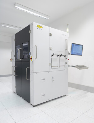
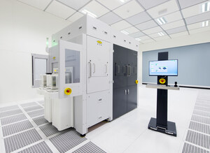
CHIBA CITY, Japan, Dec. 6, 2011 /PRNewswire/ -- SEMICON JAPAN -- EV Group (EVG), a leading supplier of wafer bonding and lithography equipment for the MEMS, nanotechnology and semiconductor markets, today announced that Asahi Kasei E-Materials Corporation, the core operating company of the Asahi Kasei Group for electronics materials, energy materials, photosensitive materials and epoxy resins, has purchased an IQ Aligner UV nanoimprint lithography (UV-NIL) system from EVG. The IQ Aligner, a flexible platform designed to enable multiple steps in the manufacture of wafer-level cameras, will be used by Asahi Kasei to develop materials critical for enabling high-resolution wafer-level optics (which are used in a wide variety of applications, such as smart phones and pico projectors).
"As a leading provider of high-clarity, high-heat-resistant materials for optical and display components used in mobile electronics equipment, Asahi Kasei places great importance on research and development of new materials to better serve the rapidly growing mobile device market," stated Mr. Shoichi Furukawa, General Manager, Electronics Materials Division, for Asahi Kasei. "We purchased EVG's IQ Aligner to support our research and development efforts because it is the de-facto industry standard for UV-NIL, which is a critical enabler of wafer-level optics. We anticipate that the IQ Aligner, and the close cooperation with EVG's process teams, will significantly contribute to our development of new and unique materials that will help enable our customers' next-generation products."
In wafer-level camera production, glass substrates are typically used as carrier and spacer wafers for the lenses, which are composed of an optical polymer material. The different material characteristics of these components limit resolution and picture quality, which hinder the scalability and quality of the camera modules. EVG's Monolithic Lens Molding (MLM) process—an option available on its IQ Aligner system—overcomes this limitation by eliminating the need for glass substrates. Instead, the polymer is molded between two stamps and then cured with UV exposure by EVG's IQ Aligner system. By omitting the glass substrates, wafer-level optics manufacturers face fewer constraints on the optic and lens stack design—enabling the production of thinner lens wafers and significantly shorter optical stacks. In addition, since the IQ Aligner molds the micro-lenses using a room-temperature UV-NIL process versus thermal imprinting, a high degree of precision alignment is achieved between the various elements in the optical lens stack—maximizing device performance.
"As the market for mobile devices continues to evolve rapidly, new solutions are needed to support the production of increasingly sophisticated wafer-level optics that are being integrated into these consumer products," stated Paul Lindner, executive technology director, EVG. "Asahi Kasei is a recognized leader in advancing materials and chemistry technology, and we are pleased that they have selected our IQ Aligner system to develop the next generation of materials that will be integrated into the advanced optical lens stacks and help fuel the growth of the wafer-level camera market."
About Asahi Kasei E-materials
Asahi Kasei E-materials is the core operating company of the Asahi Kasei Group, established in April 2009 to consolidate businesses for electronics materials, energy materials, photosensitive materials, and epoxy resins to create better value for customers through synergy of product and service.
Asahi Kasei E-materials holds dominant market share for materials such as photo sensitive polyimide "Pimel™", ultra thin glass fablic, epoxy latent curing agent "Novacure™", photosensitive dry film resist "Sunfort™", photo mask anti dust film "Pellicles™" and separator membrane for lithium-ion rechargeable batteries "Hipore™".
Asahi Kasei E-materials' R&D system enables speedy development of unique and advanced electronics materials through close attention to customer voice and collaboration with key market players.
About EV Group (EVG)
EV Group (EVG) is a world leader in wafer-processing solutions for semiconductor, MEMS and nanotechnology applications. Through close collaboration with its global customers, the company implements its flexible manufacturing model to develop reliable, high-quality, low-cost-of-ownership systems that are easily integrated into customers' fab lines. Key products include wafer bonding, lithography/nanoimprint lithography (NIL) and metrology equipment, as well as photoresist coaters, cleaners and inspection systems.
In addition to its dominant share of the market for wafer bonders, EVG holds a leading position in NIL and lithography for advanced packaging and MEMS. Along these lines, the company co-founded the EMC-3D consortium in 2006 to create and help drive implementation of a cost-effective through-silicon via (TSV) process for major ICs and MEMS/sensors. Other target semiconductor-related markets include silicon-on-insulator (SOI), compound semiconductor and silicon-based power-device solutions.
Founded in 1980, EVG is headquartered in St. Florian, Austria, and operates via a global customer support network, with subsidiaries in Tempe, Ariz.; Albany, N.Y.; Yokohama and Fukuoka, Japan; Seoul, Korea and Chung-Li, Taiwan. More information is available at www.EVGroup.com.
SOURCE EV Group


Share this article