Tokyo Institute of Technology Installs EV Group Wafer Cleaning System for Advanced Optical IC Research and Development
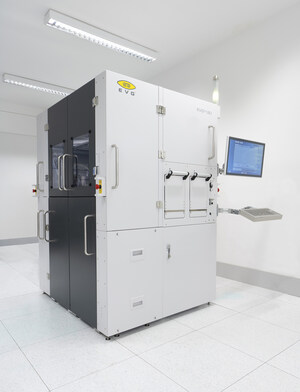
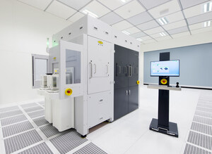
TOKYO, March 1, 2012 /PRNewswire/ -- EV Group (EVG), a leading supplier of wafer bonding and lithography equipment for the MEMS, nanotechnology and semiconductor markets, today announced that it has shipped an EVG301 semi-automated single-wafer cleaning system to Tokyo Institute of Technology (Tokyo Tech). The EVG301 has already been installed at Tokyo Tech's Arai-Nishiyama Lab, and is being used in the research and development of advanced optical communication ICs. Specifically, the EVG 301 is being leveraged by Tokyo Tech to remove particles from the surfaces of pre-bonded III-V compound semiconductor and silicon-on-insulator (SOI) wafers that are used in the production of optical ICs.
As network traffic continues to rise dramatically, the need for higher levels of integration in optical communication ICs, including the use of optical routers and wave division multiplexing (WDM) transceivers, is needed to keep transmission rates of each channel at manageable levels. In response to this need, Tokyo Tech's Arai-Nishiyama lab initiated work to develop compound semiconductor-based optical transceiver components on silicon, which enables higher levels of circuit integration. EVG's EVG301 megasonic wafer cleaning system was accepted and installed by Tokyo Tech to help accelerate this project.
Dr. Nobuhiko Nishiyama, associate professor at Arai-Nishiyama Lab, commented, "When you build optical circuits on a silicon platform, creating high-quality luminescent components is essential, and improving wafer bond quality plays an important role in making this happen. The existence of even very small particles creates voids on the wafer bonding interface, and such voids prohibit the normal performance of luminescent components. The EVG301 megasonic wafer cleaning system by EV Group completely removes such particles and enables perfect bonding results. I am confident our research will show significant progress with the use of this technology."
Today's electronics industry is built on high-speed/high-integration silicon devices. Integration of optical circuits on silicon not only improves network speed, but also increases the functionality of IC devices, including membrane photonic integrated circuits. Effective stacking of III-V compound semiconductors, such as indium phosphide (InP) and gallium indium arsenide phosphide (GaInAsP), to create high-performance optical ICs on silicon is essential to enabling such higher integration and functionality. Wafer cleaning technology, offered by EV Group, removes voids caused by particles during the wafer bonding process.
"It is our pleasure to have our EVG301 accepted by Tokyo Tech, which leads optical communication IC research and development," stated Yuichi Otsuka, representative director of EV Group Japan KK. "The EVG301 is widely used in research organizations as the de facto standard for wafer cleaning for various wafer bonding processes—and it is offered as a standard component to EVG's leading-edge, fully integrated wafer bonding systems. Tokyo Tech's selection of the EVG301 for use in their Arai-Nishiyama Lab for advanced research in high-performance semiconductor lasers and highly integrated optical ICs reaffirms the system's status as the tool of record in this field of research."
About Tokyo Institute of Technology
Tokyo Institute of Technology is the largest national university of science and technology in Japan with a 130-year history. Established as Tokyo Technical School in 1881, it became Tokyo Technical High School in 1901, which was then located in Kuramae, Tokyo, and in 1929, it acquired the university status as "Tokyo Kogyo Daigaku"' (Tokyo Institute of Technology). It has always been at the frontier of the times and played the pivotal role as a reliable leader in science and technology. Since obtaining a corporate status in 2004, Tokyo Institute of Technology has increasingly impressed people both home and abroad with the quality of education integrated with research and the unique and outstanding research projects.
About EV Group (EVG)
EV Group (EVG) is a world leader in wafer-processing solutions for semiconductor, MEMS and nanotechnology applications. Through close collaboration with its global customers, the company implements its flexible manufacturing model to develop reliable, high-quality, low-cost-of-ownership systems that are easily integrated into customers' fab lines. Key products include wafer bonding, lithography/nanoimprint lithography (NIL) and metrology equipment, as well as photoresist coaters, cleaners and inspection systems.
In addition to its dominant share of the market for wafer bonders, EVG holds a leading position in NIL and lithography for advanced packaging and MEMS. Along these lines, the company co-founded the EMC-3D consortium in 2006 to create and help drive implementation of a cost-effective through-silicon via (TSV) process for major ICs and MEMS/sensors. Other target semiconductor-related markets include silicon-on-insulator (SOI), compound semiconductor and silicon-based power-device solutions.
Founded in 1980, EVG is headquartered in St. Florian, Austria, and operates via a global customer support network, with subsidiaries in Tempe, Ariz.; Albany, N.Y.; Yokohama and Fukuoka, Japan; Seoul, Korea and Chung-Li, Taiwan. More information is available at www.EVGroup.com.
SOURCE EV Group


Share this article