EV Group Unveils Industry's First Wafer Bonding System for 450-mm Silicon-on-Insulator Semiconductor Wafers
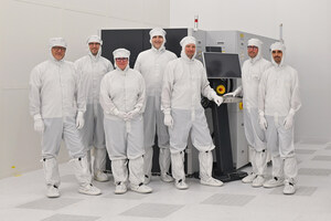
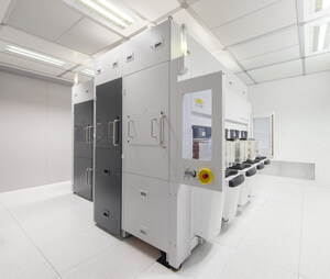
SAN FRANCISCO, Calif., July 11, 2011 /PRNewswire/ -- SEMICON WEST -- EV Group (EVG), a leading supplier of wafer bonding and lithography equipment for the MEMS, nanotechnology and semiconductor markets, today unveiled the semiconductor industry's first bonding system for 450-mm-diameter wafers manufactured from silicon-on-insulator (SOI) substrates. Building on EVG's leadership in SOI wafer bonding, the new system – dubbed the EVG850SOI/450 mm – was created to support and facilitate the industry transition to 450-mm wafers from the current 300-mm standard. Leading SOI wafer provider Soitec will install, test and qualify the first EVG850SOI/450-mm system at its Grenoble, France, headquarters. Delivery is slated for fall 2011.
(Photo: http://photos.prnewswire.com/prnh/20110711/SF32537)
For more than 40 years, Moore's Law has been the primary driver for innovation in the semiconductor industry. The benefits of reduced cost per transistor, better performance and increased functionality enable increased transistor budgets for innovative designs. Because IC cost per square centimeter (cost/cm2) approximately doubles each decade, however, the industry has undergone a coincident transition in wafer size every eight to 10 years – while continuing to scale feature sizes – in order to stay on the path of Moore's Law. SOI is expected to play an enabling role in the shift to 450 mm, as it not only answers most of the scaling challenges, but it also delivers better power/performance for sub-22-nm CMOS and 3D technologies compared to similar-geometry bulk CMOS.
Wafer bonding is a crucial technique for fabricating SOI wafers, as it enables achievement of high-quality, single-crystal silicon films on one insulating layer to form SOI substrates. The new EVG850SOI/450-mm wafer bonding system leverages EVG's strengths in wafer bonding technology to create a fully automated tool for production-level fabrication of SOI wafers. Moreover, because chipmakers will need an interim solution to optimize productivity for existing 300-mm capacity as the migration to 450 mm proceeds over the next few years, the system can serve as a bridge tool, allowing processing of both wafer sizes.
"Every bonded 300-mm SOI wafer and nearly 100 percent of all SOI wafers are fabricated on EVG systems. We delivered our first SOI bonding system in 1994, and our global installed base continues to grow with widened adoption of SOI substrates," noted EV Group Executive Technology Director Paul Lindner. "One of the most important SOI fabrication processes based on wafer bonding is the Smart CutTM layer transfer technology from Soitec, with whom EV Group has a longstanding collaborative relationship. Soitec is the ideal recipient of the first EVG 450-mm SOI wafer bonding system, and their evaluation of the alpha-tool will be invaluable for optimizing the system modules."
The EVG850SOI/450 mm consists of two process modules: a cleaning module for cleaning and pre-conditioning of wafers before wafer bonding, and an SOI pre-bonding module. In the pre-bonding module, the two silicon wafers are joined together either in a vacuum or in an atmospheric chamber. The tool is equipped with state-of-the-art 450-mm load ports and front opening unified pods (FOUPs). Most of the particle and metal ion contamination tests will be performed on 300-mm wafers due to the lack of 450-mm metrology systems. The first tool in EVG's 450-mm arsenal, the new bonder will serve as the key starting point for the production of 450-mm SOI wafers, and can be utilized for the development of other EV Group 450-mm products, such as mask aligners and coating systems. An extension of the system with additional modules is planned as a further step to increase wafer throughput.
Noted Chief Operating Officer Paul Boudre for Soitec, "Soitec is willing to position in the 450-mm transition. With the launch of this new system, EV Group is offering the semiconductor industry a highly viable solution to ease the transition to 450-mm wafers. With our well established SOI material playing an increasingly greater role in fabricating next-generation ICs, we look forward to working with EVG to ensure this new system is ready to enter mainstream production in a timely fashion."
During SEMICON West this week in San Francisco, EV Group will have representatives from its team of SOI and wafer bonding experts available in Booth #1131 to speak with press, analysts and customers interested in learning more about the new EVG850SOI/450-mm system and its capabilities for bridging and enabling the 300-mm to 450-mm wafer transition. In addition, EVG's Paul Lindner will be part of the MCA's BrightSpots Forum on 450 mm to be held this evening at 6:00 p.m. (PST)—where he will touch on some of the efforts currently under way, both collectively and individually, to enhance 300-mm manufacturing efficiency as well as enable the industry's transition to 450-mm wafers. This event is open to the media and is accessible online, allowing participants a unique opportunity to gain greater insight into the challenges and opportunities associated with 450 mm, and pose questions directly to some of the foremost experts in the field. To register for online access to the live panel event, click here: https://www2.gotomeeting.com/register/378232715.
About EV Group
EV Group (EVG) is a world leader in wafer-processing solutions for semiconductor, MEMS and nanotechnology applications. Through close collaboration with its global customers, the company implements its flexible manufacturing model to develop reliable, high-quality, low-cost-of-ownership systems that are easily integrated into customers' fab lines. Key products include wafer bonding, lithography/nanoimprint lithography (NIL) and metrology equipment, as well as photoresist coaters, cleaners and inspection systems.
In addition to its dominant share of the market for wafer bonders, EVG holds a leading position in NIL and lithography for advanced packaging and MEMS. Along these lines, the company co-founded the EMC-3D consortium in 2006 to create and help drive implementation of a cost-effective through-silicon via (TSV) process for major ICs and MEMS/sensors. Other target semiconductor-related markets include silicon-on-insulator (SOI), compound semiconductor and silicon-based power-device solutions.
Founded in 1980, EVG is headquartered in St. Florian, Austria, and operates via a global customer support network, with subsidiaries in Tempe, Ariz.; Albany, N.Y.; Yokohama and Fukuoka, Japan; Seoul, Korea and Chung-Li, Taiwan. The company's unique Triple i-approach (invent - innovate - implement) is supported by a vertical integration, allowing EVG to respond quickly to new technology developments, apply the technology to manufacturing challenges and expedite device manufacturing in high volume. More information is available at www.EVGroup.com.
SOURCE EV Group
WANT YOUR COMPANY'S NEWS FEATURED ON PRNEWSWIRE.COM?
Newsrooms &
Influencers
Digital Media
Outlets
Journalists
Opted In


Share this article