EV Group Adds In-Line Metrology Capability to Wafer Bonding Systems to Support High-Volume 3D-IC and TSV Manufacturing
First-ever Integration of In-line Metrology with Temporary Bonding/Debonding Enables More Repeatable and Reliable Process, Improved Yields and Lower Cost of Production
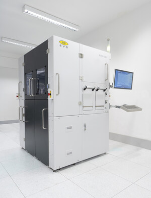
ST. FLORIAN, Austria, June 21, 2011 /PRNewswire/ -- EV Group (EVG), a leading supplier of wafer bonding and lithography equipment for the MEMS, nanotechnology and semiconductor markets, today announced it has introduced a new in-line metrology module for its EVG850TB automated temporary bonding and debonding systems. This new metrology capability, which is now available as an option on the EVG850TB and EVG850DB platforms, allows customers to implement in-line process control for thin-wafer processing. This enables IC manufacturers to reduce defects and wafer breakage—thereby improving yields and lowering production costs. Adding in-line metrology to thin-wafer processing is particularly crucial in helping to enable the ramp-up of 3D-IC and TSV manufacturing from pilot-line to volume production.
EVG's new integrated in-line metrology module can detect a variety of process irregularities and defects during temporary bonding and debonding, including: total thickness variation (TTV) of the carrier wafer, adhesive layer, bonded stack and thinned wafer; bow/warp of the bonded stack; and voids in the bond interface.
With semiconductor device scaling reaching its physical limits and becoming increasingly cost prohibitive, IC manufacturers are turning to 3D IC architectures—where multiple circuit layers are stacked into a single circuit and connected via TSVs—in order to increase device functionality. Thin-wafer processing is key to enabling TSV applications. However, since thin wafers are very fragile and prone to breakage, temporary bonding of the device wafer to a carrier wafer is needed to provide stability to the device wafer during thin-wafer processing. After thinning and backside processing, the device wafer must then be debonded in order for the individual devices to be singulated and packaged.
Since device wafers undergo many process steps prior to thin-wafer processing, it is essential that the wafer thinning and bonding/debonding process do not contribute to yield loss. By integrating in-line metrology into its EVG850TB/DB platforms—the industry standard for temporary wafer bonding and debonding—EVG has provided its customers with a powerful new tool to optimize their wafer-thinning and bonding processes, reduce tool downtime resulting from yield issues that arise during processing, and maximize their product yields and investments.
"For more than 10 years, EV Group has pioneered thin-wafer processing with our temporary bonding and debonding solutions—continuously adding new features that enable our customers to aggressively pursue their technology roadmaps and lower their cost of production," stated Dr. Thorsten Matthias, Business Development Director at EVG. "With our new integrated in-line metrology module, we can now provide a total solution for thin-wafer processing that will enable our customers to reach the next level of production readiness on their leading-edge products by giving them overall control of their entire metrology process, including setting control values to help mitigate the cumulative effects of any bonding/debonding process issues."
Added Matthias, "Beyond improving yields, the integration of in-line metrology to our EVG850TB/DB systems can also enable temporary bonding and debonding to be performed by different companies—opening up an entirely new supply chain model for TSV manufacturing to further increase TSV adoption and drive down costs. Integrated device manufacturers (IDMs) and foundries can now perform temporary bonding, thinning and backside processing, while outsourced semiconductor assembly and test (OSAT) companies can do the debonding before dicing and packaging—since each party can perform outgoing or incoming qualification of the integrity of these extremely fragile thin wafers."
As part of its ongoing efforts to share its expertise and educate customers and partners regarding its 3D technology capabilities, EV Group will be presenting at two upcoming industry conferences. Markus Wimplinger, corporate technology development and IP director, will speak on "In-line IR metrology for high-volume temporary bonding applications" at the SEMATECH Workshop on 3D Interconnect Technology, July 13, 2011, in San Francisco, Calif.; and Thorsten Matthias, director of business development, will present on "Thin die stacking for wide I/O interface memory-on-logic" during SEMICON Europa, October 11-13, 2011, in Dresden, Germany.
About EV Group
EV Group (EVG) is a world leader in wafer-processing solutions for semiconductor, MEMS and nanotechnology applications. Through close collaboration with its global customers, the company implements its flexible manufacturing model to develop reliable, high-quality, low-cost-of-ownership systems that are easily integrated into customers' fab lines. Key products include wafer bonding, lithography/nanoimprint lithography (NIL) and metrology equipment, as well as photoresist coaters, cleaners and inspection systems.
In addition to its dominant share of the market for wafer bonders, EVG holds a leading position in NIL and lithography for advanced packaging and MEMS. Along these lines, the company co-founded the EMC-3D consortium in 2006 to create and help drive implementation of a cost-effective through-silicon via (TSV) process for major ICs and MEMS/sensors. Other target semiconductor-related markets include silicon-on-insulator (SOI), compound semiconductor and silicon-based power-device solutions.
Founded in 1980, EVG is headquartered in St. Florian, Austria, and operates via a global customer support network, with subsidiaries in Tempe, Ariz.; Albany, N.Y.; Yokohama and Fukuoka, Japan; Seoul, Korea and Chung-Li, Taiwan. The company's unique Triple i-approach (invent - innovate - implement) is supported by a vertical integration, allowing EVG to respond quickly to new technology developments, apply the technology to manufacturing challenges and expedite device manufacturing in high volume. More information is available at www.EVGroup.com.
SOURCE EV Group


Share this article