New Wafer-Level Microlens Molding Process From EV Group Extends Manufacturing Roadmap for CMOS Image Sensors
New Monolithic Lens Molding (MLM) capability enables up to eight-megapixel-and-higher-resolution devices
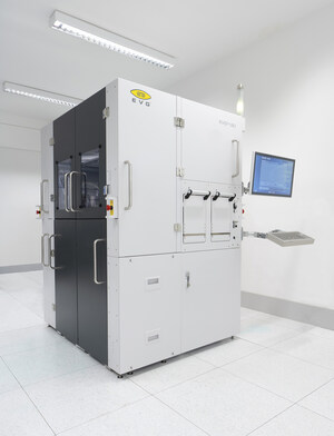
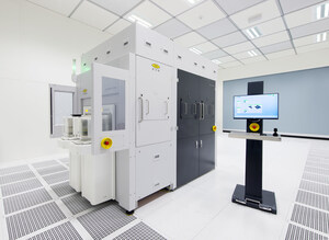
CHIBA, Japan, Dec. 1, 2010 /PRNewswire/ -- SEMICON JAPAN -- EV Group (EVG), a leading supplier of wafer bonding and lithography equipment for the MEMS, nanotechnology and semiconductor markets, today announced that it has developed a new micro-lens molding process that can enable volume production of very-high-resolution (up to eight megapixels and higher) wafer-level optics for use in smart phones, pico projectors and myriad other applications. The new Monolithic Lens Molding (MLM) capability, which was developed in-house by EVG's process development team, is available as an option on the company's IQ Aligner UV nanoimprint lithography (UV-NIL) system or can be upgraded to existing equipment. EVG expects to ship its first IQ Aligner with the MLM option in the first half of 2011.
As the size of the camera in mobile phones can be a limiting factor in mobile handset designs, there is an increasing demand for smaller camera modules that can still address the call for higher resolution and cost effectiveness. This has shifted manufacturing of both the CMOS image sensor and the micro-optics stack to the wafer level. At the same time, the evolution of wafer-level cameras toward higher pixel counts to meet higher performance standards is driving the need for more complex optical systems and, consequently, tighter manufacturing tolerances.
In wafer-level camera production today, glass substrates are typically used as carrier and spacer wafers for the lenses, which are composed of an optical polymer material. The different material characteristics of these components limit resolution and picture quality, which hinder the scalability and quality of the camera modules. EVG's MLM process overcomes this limitation by eliminating the need for glass substrates. Instead, the polymer is molded between two stamps and then cured with UV exposure by the EVG's IQ Aligner system. By omitting the glass substrates, wafer-level optics manufacturers face fewer constraints on the optic and lens stack design—enabling the production of thinner lens wafers and significantly shorter optical stacks. In addition, since the IQ Aligner molds the micro-lenses using a room-temperature UV-NIL process versus thermal imprinting, a high degree of precision alignment is achieved between the various elements in the optical lens stack—maximizing device performance.
Markus Wimplinger, corporate technology development and IP director of EV Group, noted, "Given the incredibly dynamic nature of the wafer-level camera market, manufacturers need solutions that can give them a clear competitive edge. Leading-edge technology and process know-how are both important considerations in choosing the right equipment vendors to partner with in supporting their manufacturing efforts. Our new MLM option extends our wafer-level micro-lens manufacturing capabilities to afford our customers more flexibility in their designs and support their production roadmaps. As the first equipment supplier to offer a production-ready process for monolithic lens molding, this latest offering from EV Group further cements our leadership in the wafer-level camera market."
Those interested in learning more about the new MLM option on the IQ Aligner and EVG's broad portfolio of wafer bonding and lithography equipment are invited to visit the company in booth #4A-507 during SEMICON Japan, December 1-3, at Makuhari Messe in Chiba, Japan.
In other news, EVG recently announced that the company witnessed a more than 20-percent increase in overall revenue during fiscal 2010, ended September 30. EVG attributes this growth, in large part, to continued demand for equipment used in advanced manufacturing of 3D ICs, CMOS image sensors and MEMS devices. In fact, the company reports it has grown, on average, approximately 20 percent year-over-year since 2003-successfully avoiding a drop in order intake and revenue even in 2008 and 2009 despite the global economic recession.
About EV Group
EV Group (EVG) is a world leader in wafer-processing solutions for semiconductor, MEMS and nanotechnology applications. Through close collaboration with its global customers, the company implements its flexible manufacturing model to develop reliable, high-quality, low-cost-of-ownership systems that are easily integrated into customers' fab lines. Key products include wafer bonding, lithography/nanoimprint lithography (NIL) and metrology equipment, as well as photoresist coaters, cleaners and inspection systems.
In addition to its dominant share of the market for wafer bonders, EVG holds a leading position in NIL and lithography for advanced packaging and MEMS. Along these lines, the company co-founded the EMC-3D consortium in 2006 to create and help drive implementation of a cost-effective through-silicon via (TSV) process for major ICs and MEMS/sensors. Other target semiconductor-related markets include silicon-on-insulator (SOI), compound semiconductor and silicon-based power-device solutions.
Founded in 1980, EVG is headquartered in St. Florian, Austria, and operates via a global customer support network, with subsidiaries in Tempe, Ariz.; Albany, N.Y.; Yokohama and Fukuoka, Japan; Seoul, Korea and Chung-Li, Taiwan. The company's unique Triple i-approach (invent - innovate - implement) is supported by a vertical integration, allowing EVG to respond quickly to new technology developments, apply the technology to manufacturing challenges and expedite device manufacturing in high volume. More information is available at www.EVGroup.com.
SOURCE EV Group


Share this article