Fraunhofer IZM-ASSID Selects EV Group Temporary Bonding and Debonding Equipment for Developing Processes for High-Volume Manufacturing of 3D ICs
EVG Systems Selected for Platform Flexibility, Functionality and Industry-Proven Reliability
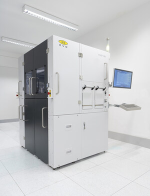
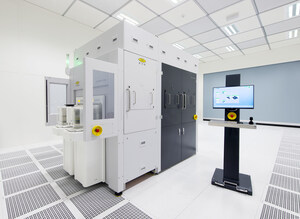
ST. FLORIAN, Austria, May 31 /PRNewswire/ -- EV Group (EVG), a leading supplier of wafer bonding and lithography equipment for the MEMS, nanotechnology and semiconductor markets, today announced that world-renowned research institute, Fraunhofer IZM-ASSID, has placed an order for two EVG temporary bonding and debonding (TB/DB) systems for thin-wafer handling and processing for 3D ICs. ASSID (All Silicon System Integration Dresden), a new project group of Fraunhofer IZM, will use EVG's systems for advanced 3D wafer-level process integration flow development for Fraunhofer's industrial partners. Both EVG systems will be installed later this year at ASSID's state-of-the-art facility in Dresden—the first Fraunhofer Center with a 300-mm line dedicated to developing processes for high-volume manufacturing of 3D ICs.
This latest order from Fraunhofer IZM-ASSID bolsters EVG's market-leading installed base of temporary bonding and debonding systems—currently totaling more than 60 system installations worldwide.
3D IC technology is gaining momentum as the technology of choice in addressing consumer demand for smaller, lower-power electronic devices with greater functionality. However, unlike manufacturing conventional ICs, which are built on silicon wafers approximately 750-microns thick, 3D ICs require the use of much thinner wafers of about 100 microns or less. Given the inherent fragility of these ultra-thin wafers, thin-wafer processing requires TB/DB technology to ensure the structural integrity of the wafer—particularly when it undergoes high-temperature, high-stress processes such as etching and metallization. By temporarily bonding the ultra-thin wafer to a carrier substrate and then leveraging a stress-free debonding approach after back side processing, TB/DB technology offers integrity-assured processing, which results in higher yield. EVG's industry-proven TB/DB technology is designed to support a wide variety of processes—including those already established and in industrial use today, as well as those outlined in roadmap requirements for future 3D device generations.
"At Fraunhofer IZM-ASSID, we develop highly tailored processes for leading semiconductor manufacturers with very different requirements, and we need flexible and scalable process solutions to meet a wide variety of needs," said Jurgen Wolf, manager and coordinator of ASSID. "EV Group's temporary bonding and debonding platforms enable seamless development and evolution of the 3D integration processes and technologies for our customers. The success we have had with previous EV Group systems, combined with superior demo results and EVG's overall process expertise in 3D packaging, were all key factors in our selection criteria for this order."
"This is a very important win for EV Group, as Fraunhofer is one of the premiere research facilities in Europe dedicated to 3D IC technology advancement," noted EV Group executive technology director, Paul Lindner. "This marks another step forward in establishing EV Group's technology solutions as the industry standard for wafer-level packaging applications, particularly 3D ICs. We look forward to a mutually beneficial cooperation with Fraunhofer IZM and its ASSID project, and taking our industry-leading technology and process expertise in 3D packaging to a new level."
The wafer bonding and thin-wafer handling equipment market represents another high-growth segment in which EVG has successfully established its technology process and expertise. Its dominant position in this market contributed to EVG's financial success in 2009, when the company continued to see an increase in both order intake and revenue despite the global economic recession.
EVG and Fraunhofer-IZM are both members of the EMC-3D Consortium, where they have collaborated closely, along with other consortium members, on lowering 3D IC manufacturing costs to incite greater technology adoption.
About Fraunhofer IZM-ASSID
Fraunhofer IZM has long-term experience in wafer level packaging and system integration technologies, especially with respect to 3D integration. New wafer level processes are developed and new materials are evaluated and implemented into a complete process integration flow. Upgrading 3D wafer level technologies to 300-mm wafer size is the next step in effectively assisting leading companies in meeting the performance, functionality and scaling requirements of their future products. "All Silicon System Integration Dresden" (ASSID) has been established as part of the Fraunhofer IZM Berlin to meet this specific challenge. Our new center has a state-of-the-art clean-room facility and is equipped with a complete 300-mm process line for TSV formation, TSV post-processing on wafer frontside and backside, 3D device stacking assembly, as well as testing and failure analysis. All these ASSID activities are embedded into the overall Fraunhofer IZM's 3D system integration strategy. ASSID's facilities and know-how are especially tailored to partners in industry for research and development projects, as well as prototype realization. We are also establishing a network for advanced system integration technologies together with other research institutes and universities.
About EV Group
EV Group (EVG) is a world leader in wafer-processing solutions for semiconductor, MEMS and nanotechnology applications. Through close collaboration with its global customers, the company implements its flexible manufacturing model to develop reliable, high-quality, low-cost-of-ownership systems that are easily integrated into customers' fab lines. Key products include wafer bonding, lithography/nanoimprint lithography (NIL) and metrology equipment, as well as photoresist coaters, cleaners and inspection systems.
In addition to its dominant share of the market for wafer bonders, EVG holds a leading position in NIL and lithography for advanced packaging and MEMS. Along these lines, the company co-founded the EMC-3D consortium in 2006 to create and help drive implementation of a cost-effective through-silicon via (TSV) process for major ICs and MEMS/sensors. Other target semiconductor-related markets include silicon-on-insulator (SOI), compound semiconductor and silicon-based power-device solutions.
Founded in 1980, EVG is headquartered in St. Florian, Austria, and operates via a global customer support network, with subsidiaries in Tempe, Ariz.; Albany, N.Y.; Yokohama and Fukuoka, Japan; Seoul, Korea and Chung-Li, Taiwan. The company's unique Triple i-approach (invent - innovate - implement) is supported by a vertical integration, allowing EVG to respond quickly to new technology developments, apply the technology to manufacturing challenges and expedite device manufacturing in high volume. More information is available at www.EVGroup.com.
SOURCE EV Group


Share this article