EV Group Wins Order for UV-NIL/Hot Embossing Systems from Fraunhofer Research Institution for Electronic Nano Systems
New Customer Fraunhofer ENAS to Implement Advanced Lithography R&D Using EVG's Tools with New SMS-NIL Technology for Ultra-high-resolution Patterning
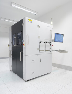
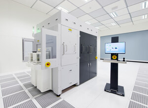
DRESDEN, Germany, Oct. 19 /PRNewswire/ -- SEMICON EUROPA – EV Group (EVG), a leading supplier of wafer bonding and lithography equipment for the MEMS, nanotechnology and semiconductor markets, today announced receipt of its first order from the Fraunhofer Research Institution for Electronic Nano Systems ENAS (Chemnitz, Germany). Fraunhofer ENAS purchased an EVG6200NT automated mask aligner and an EVG540 automated wafer bonder, and will employ the flexible, multi-process EVG systems for mask lithography, ultraviolet nanoimprint lithography (UV-NIL), bond alignment, bonding and hot embossing (HE). The systems, which will enable Fraunhofer ENAS to process product wafers up to 200 mm in diameter, are slated for delivery in early November.
Fraunhofer ENAS closely cooperates with Chemnitz University of Technology's Center for Microtechnologies—running a state-of-the-art cleanroom facility. The institute works closely with major customers worldwide, focusing its industrial research on MEMS/NEMS, back-end-of-line (BEOL) micro and nano electronics processes, 3D IC integration and reliability. According to Dr. Thomas Gessner, a professor and director at Fraunhofer ENAS, a primary reason the prestigious institution selected the EVG systems is the advanced technology capabilities they afford. "NIL and hot embossing are key processes for extending our advanced R&D efforts," said Professor Gessner. "The EVG systems allow us to implement these technologies far better than competitive tools. We can now perform full-area nanoimprints, as well as optically aligned UV-NIL and HE, on larger wafers, further expanding our ability to support a broad spectrum of processes."
EVG's recently announced soft molecular scale UV-NIL, or SMS-NIL, technology patterns ultra-high-resolution features down to 12.5 nm on EVG's proven UV-NIL systems. The technology uses soft polymeric working stamps to avoid damaging costly master stamps, resulting in significantly lower processing costs compared to other nano-patterning techniques. EVG reports that SMS-NIL is already used in industrial environments for CMOS image sensors, micro-lens molding and other optical applications.
"This order from a leading research partner such as Fraunhofer ENAS underscores the value of our ongoing efforts to develop and implement new, leading-edge technologies that compliment and extend the applications for our systems," said Markus Wimplinger, EVG's corporate technology development and IP director. "Not only will our tools' flexibility allow Fraunhofer ENAS to perform multiple lithography, alignment and bonding processes on just two systems, but through close cooperation between both companies, processes such as EVG's unique SMS-NIL technology, as well as hot embossing processes, will be implemented and further advanced."
Further supporting its expertise in the MEMS arena, EVG announced another key order for the MEMS market today—Norway-based MEMS sensor producer Sensonor Technologies AS ordered an EVG Gemini for thermal imaging manufacturing. EVG also added another bonder to its arsenal, rolling out the new EVG®520L3 semi-automated, high-vacuum wafer bonding system for applications including metal bonding for 3D IC, MEMS, and CMOS compatibility.
Those interested in learning more about EVG's SMS-NIL technology and broad portfolio of wafer bonding and lithography equipment are invited to visit the company in booth #1568 (Hall 1) during SEMICON Europa, October 19-21, 2010, at Messe Dresden, Dresden, Germany.
About EV Group
EV Group (EVG) is a world leader in wafer-processing solutions for semiconductor, MEMS and nanotechnology applications. Through close collaboration with its global customers, the company implements its flexible manufacturing model to develop reliable, high-quality, low-cost-of-ownership systems that are easily integrated into customers' fab lines. Key products include wafer bonding, lithography/nanoimprint lithography (NIL) and metrology equipment, as well as photoresist coaters, cleaners and inspection systems.
In addition to its dominant share of the market for wafer bonders, EVG holds a leading position in NIL and lithography for advanced packaging and MEMS. Along these lines, the company co-founded the EMC-3D consortium in 2006 to create and help drive implementation of a cost-effective through-silicon via (TSV) process for major ICs and MEMS/sensors. Other target semiconductor-related markets include silicon-on-insulator (SOI), compound semiconductor and silicon-based power-device solutions.
Founded in 1980, EVG is headquartered in St. Florian, Austria, and operates via a global customer support network, with subsidiaries in Tempe, Ariz.; Albany, N.Y.; Yokohama and Fukuoka, Japan; Seoul, Korea and Chung-Li, Taiwan. The company's unique Triple i-approach (invent - innovate - implement) is supported by a vertical integration, allowing EVG to respond quickly to new technology developments, apply the technology to manufacturing challenges and expedite device manufacturing in high volume. More information is available at www.EVGroup.com.
SOURCE EV Group


Share this article