EV Group Launches New Flagship Model in Its GEMINI® FB Family of Fusion Wafer Bonding Systems to Enhance Throughput and Automation Performance
New Gemini FB Platform Extension Increases Throughput to Up to 20 Wafers Per Hour to Support High-volume CMOS Image Sensor and 3D Integration Applications
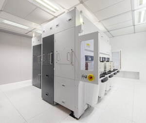
TAIPEI, Taiwan, Sept. 7, 2011 /PRNewswire/ -- SEMICON Taiwan -- EV Group (EVG), a leading supplier of wafer bonding and lithography equipment for the MEMS, nanotechnology and semiconductor markets, today announced that it is launching a new flagship model in its field-proven GEMINI FB fusion wafer bonding family that increases system throughput to up to 20 wafers per hour. The upgrade includes enhanced automation capabilities to enable customers to achieve higher levels of manufacturing efficiency for such applications as backside illuminated (BSI) CMOS image sensors, 3D integration of CMOS image sensors, and monolithic 3D integration of memory devices.
(Photo: http://photos.prnewswire.com/prnh/20110907/SF63175)
EVG's GEMINI FB system is designed for integrated and automated wafer loading, alignment, bonding and unloading of bonded wafers up to 300 mm in diameter. The company reports that it has already received orders from major integrated device manufacturers for the upgraded platform, with deliveries slated for the end of this calendar year.
According to Paul Lindner, executive technology director for EVG, "We continue to see demand among our customers for higher yields and throughput in order to maximize their return on investment. At EVG, our vision is to be the first in exploring new techniques to achieve these gains—enabling us to address next-generation applications that leverage micro and nanofabrication technologies. As part of that vision, we continually focus on innovating our product lines with enhancements such as this latest extension to our flagship GEMINI FB platform—the industry's first field-proven 300-mm fusion wafer bonding system readily available."
These latest enhancements to boost the throughput of the GEMINI FB platform are part of EVG's corporate initiative to implement 300-mm Prime standards across many of its industry-leading equipment platforms. Specifically, EVG incorporated a local material buffer, which more than doubles the number of FOUPs (front opening unified pods) on the system to 10 for continuous mode operation. EVG also employed a new, faster wafer handling system in the GEMINI FB platform—using double-end effectors on the robotic system compared to single-end effectors.
A key feature of the GEMINI FB platform includes low temperature plasma activation, which enables low temperature (<400 degrees Celcius) wafer bonding and stress/damage free annealing—a critical element for CMOS image sensor and 3D integration applications. EVG also enhanced its proprietary SmartView® technology, which allows for universal bond alignment for face-to-face, backside, infrared and transparent alignment of wafers up to 300 mm with varying thickness and materials—delivering the best alignment accuracy available today. Enhancements to the SmartView alignment system include new software that optimizes process sequences and speed. With these combined enhancements to the GEMINI FB platform, EVG has demonstrated a 26-percent increase in throughput—resulting in speeds of up to 18-20 wafer bonds per hour, depending on chamber configuration, customer applications and process recipes.
EVG will be exhibiting at SEMICON Taiwan, which will be held September 7-9, 2011 in Taipei, Taiwan. Media and analysts interested in learning more about the company and its recent developments are encouraged to visit EVG's booth #2506. In addition, several EVG executives will be presenting during the three-day long event. Visit www.semicontaiwan.org/en/ for more information.
About EV Group (EVG)
EV Group (EVG) is a world leader in wafer-processing solutions for semiconductor, MEMS and nanotechnology applications. Through close collaboration with its global customers, the company implements its flexible manufacturing model to develop reliable, high-quality, low-cost-of-ownership systems that are easily integrated into customers' fab lines. Key products include wafer bonding, lithography/nanoimprint lithography (NIL) and metrology equipment, as well as photoresist coaters, cleaners and inspection systems.
In addition to its dominant share of the market for wafer bonders, EVG holds a leading position in NIL and lithography for advanced packaging and MEMS. Along these lines, the company co-founded the EMC-3D consortium in 2006 to create and help drive implementation of a cost-effective through-silicon via (TSV) process for major ICs and MEMS/sensors. Other target semiconductor-related markets include silicon-on-insulator (SOI), compound semiconductor and silicon-based power-device solutions.
Founded in 1980, EVG is headquartered in St. Florian, Austria, and operates via a global customer support network, with subsidiaries in Tempe, Ariz.; Albany, N.Y.; Yokohama and Fukuoka, Japan; Seoul, Korea and Chung-Li, Taiwan. More information is available at www.EVGroup.com.
SOURCE EV Group
WANT YOUR COMPANY'S NEWS FEATURED ON PRNEWSWIRE.COM?
Newsrooms &
Influencers
Digital Media
Outlets
Journalists
Opted In


Share this article